IBM hails new 'block of flats' design breakthrough for ultra tiny chips
Summary
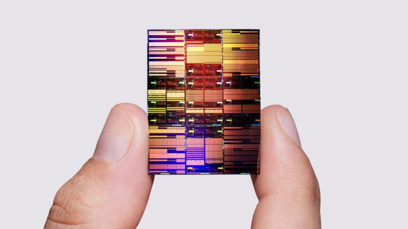
IBM has created a new design for computer chips that fits nearly 100 billion tiny switches called transistors on a chip the size of a fingernail. This chip technology uses a 0.7 nanometer scale, smaller than the current standard of 2 nanometers, aiming to improve chip power and energy use, but it may take several years before it is ready for use.Key Facts
- IBM's new chip design uses a scale of about 0.7 nanometers, smaller than the current 2-nanometer chips on the market.
- The prototype chip has nearly 100 billion transistors on a tiny silicon surface about the size of a fingernail.
- Testing shows the new chip is 50% faster and 70% more energy efficient than IBM’s 2-nanometer chip.
- The design stacks transistors in layers, like a tall building instead of spreading them flat, to fit more on a small chip.
- This approach is called NanoStack and was described as a major step forward by IBM’s research director.
- Transistors are the tiny switches that control electrical signals and determine how powerful and efficient a chip is.
- Making chips smaller and stacking transistors in 3D helps keep improving performance even as traditional chip shrinking faces limits.
- Challenges with 3D chips include managing heat and ensuring layers don’t interfere with how transistors switch off.
Read the Full Article
This is a fact-based summary from The Actual News. Click below to read the complete story directly from the original source.